


Inquiry
Cart
SEMI/PCB Measurement - Precision Inspection, Quality Control
SEMI/PCB Measurement - Precision Inspection, Quality Control
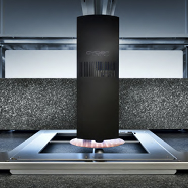
CT 600ST
Cyber Non-contact Profilometer

CT 600ST
- Dual Non-Contact Measurement System For Large Parts.
- 3d mapping of thickness,bow, warpage and rouhgness。
- User friendly concept。
- Sophisticated analysis and automation software。
- 【Applicable Range】 Typical applications for the CT 600ST are the analysis and quality control of large parts, such as large wafers, PCBs, substrates, glas and other optical components.<br> Thickness, geometry and position measurement of highly contoured objects like lenses, gaskets, turbine blades, as well as flatness and coplanarity analysis are other popular applications.
- 【Application】 Total thickness variation (TTV)、Flatness, warpage and bow、Printed products, systems or devices、Panel level packaging devices、Fuel cell elements、Medical devices.
Product Description
Other Product Description
CT 600ST
 Dual Non-Contact Measurement System For Large Parts
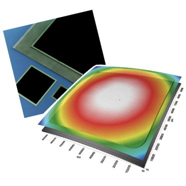 Thickness of a Fuel Cell Component
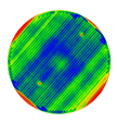
 Wafer Thickness Map(TTV)t
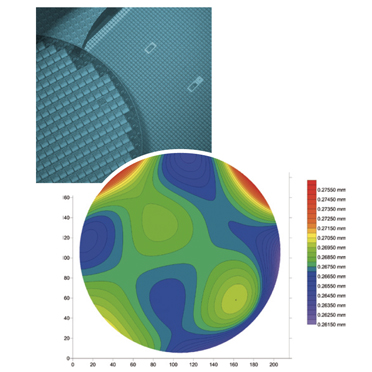
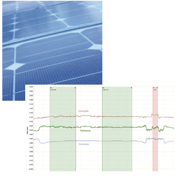 Front-and Backside Metallization of a Solar Cell
 Cyber Technologies Vantage