Inquiry
Cart
Laser Equipment - Precision Processing, Innovative Technology
Laser Equipment - Precision Processing, Innovative Technology
Wafer Laser Grooving
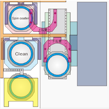
Semiconductor Industry

Wafer Laser Grooving
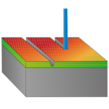
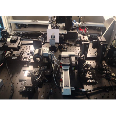
In laser processing applications, using laser for wafer grooving is superior to blade dicing which can cause PI tearing defects. Short pulse lasers can more effectively control thermal energy, reducing the impact on processing quality.
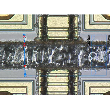
- Groove width:35-70um
- Groove Depth:>10-15um
- HAZ (Heat Affected Zone):<±2um
- Kerf check on fly function (Real time kerf aliment): Yes & 0 sec/check
- Kerf Offset adjust criteria
- 0-0.5 um : No Action
- 0.5-1 um : Automatic Corrective Acti
- >1 um : Manual Mode
Product Description
Other Product Description