


Inquiry
Cart
SEMI/PCB Measurement - Precision Inspection, Quality Control
SEMI/PCB Measurement - Precision Inspection, Quality Control
CT 300
Cyber Non-contact Profilometer

CT 300
- 2D/3D non-contact profiling system[measuring]3D (x, y, z)2D (y, z or x, z), Height, Height (Avg), Length, Volume, Angle, Angle (Planar), Center, Roughness, Radius (Avg, Max, RMS, Rz), Roughness (Avg, Max, RMS, Rz).
- Laser non-contact measurement applicable to both dry and wet films.
- Multi-points automatic measurement available with analysis result.
- 【Applicable Range】 Thickness measurement of thick film printing, hybrid circuits, BGA, TAB and FLIP CHIP.
- 【Application】 PCB substrate deformation, quality inspection of semiconductor components and wafers, measurement of thickness and roughness of copper clad laminate, thickness of solder mask and silkscreen, bump inspection, flatness measurement of die attachment, 12"wafer warpage.
Product Description
Other Product Description
CT 300
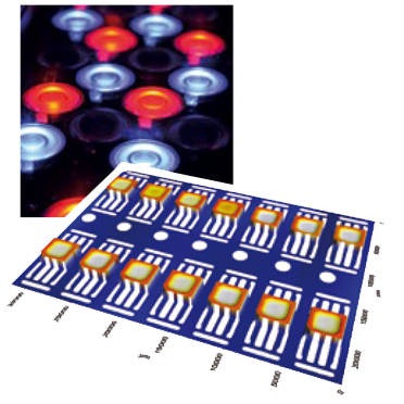 Geometry of LED devices
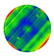
 Flatness of a silicon wafer
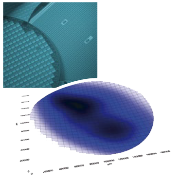
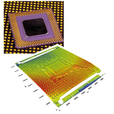 Warpage of electronic componets
 Cyber Technologies Vantage