


Inquiry
Cart
SEMI/PCB Measurement - Precision Inspection, Quality Control
SEMI/PCB Measurement - Precision Inspection, Quality Control
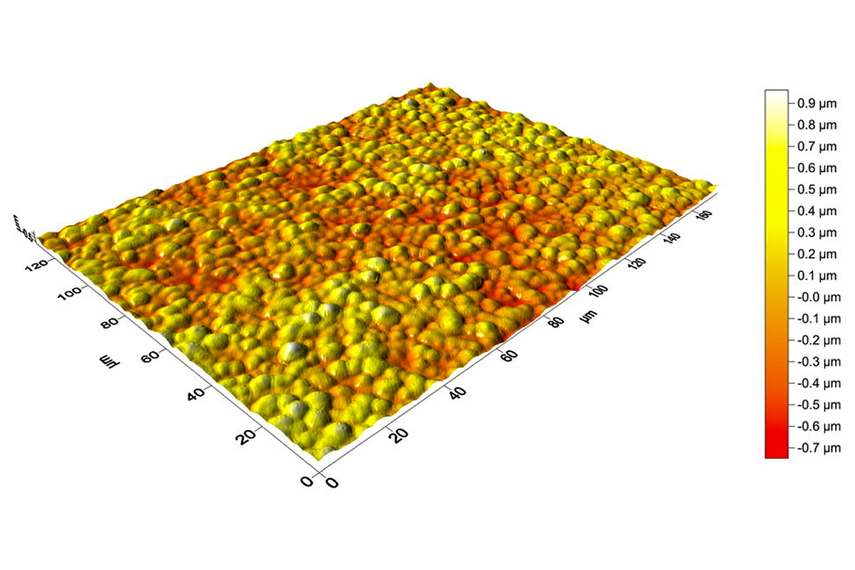
SURFACE ROUGHNESS
Cyber Non-contact Profilometer
SURFACE ROUGHNESS
- Controlling the thickness of various print layers on hybrid substrates is essential because electrical parameters are directly related to the thickness. cyberTECHNOLOGIES high resolution non-contact 3D measurement systems are the ideal tool for thickfilm measurements.
- 【Application】 ct-100、ct-R200、ct-300
Product Description
Other Product Description
 SURFACE ROUGHNESS
- Non-contact and fast surface roughness measurement according to international standards.
 GLAS, MIRRORS, WAFERS(1)
- Head-up display automotive
- WLI is ideal for smooth and super smooth surfaces
- Wafers, mirrors, glass etc.
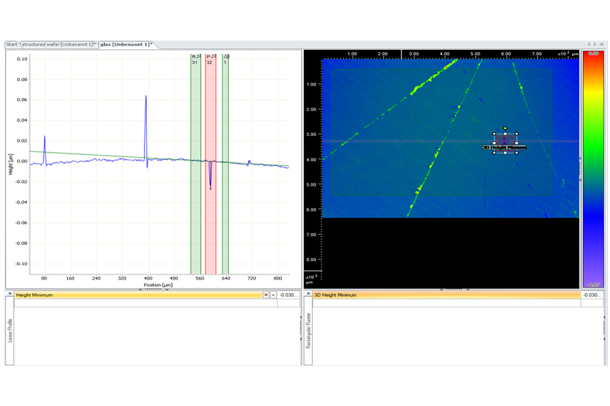 GLAS, MIRRORS, WAFERS(2)
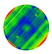
- Glas surface with scratch
- Resolution in z down to 0.1 nm
- Lateral resolution in down to 0.23 µm
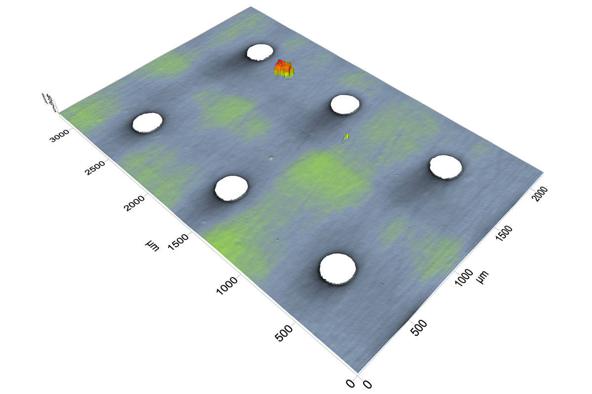 SURFACE DEFECT DETECTION(1)
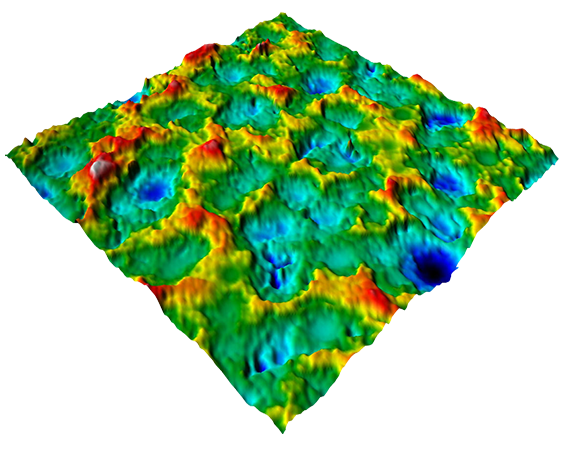
- Surface on a copper surface defect
- Find defects or particels automatically
- Measures height, position and size of defects
- User independent and accurate defect qualification
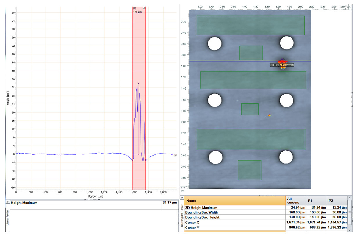 SURFACE DEFECT DETECTION(2)
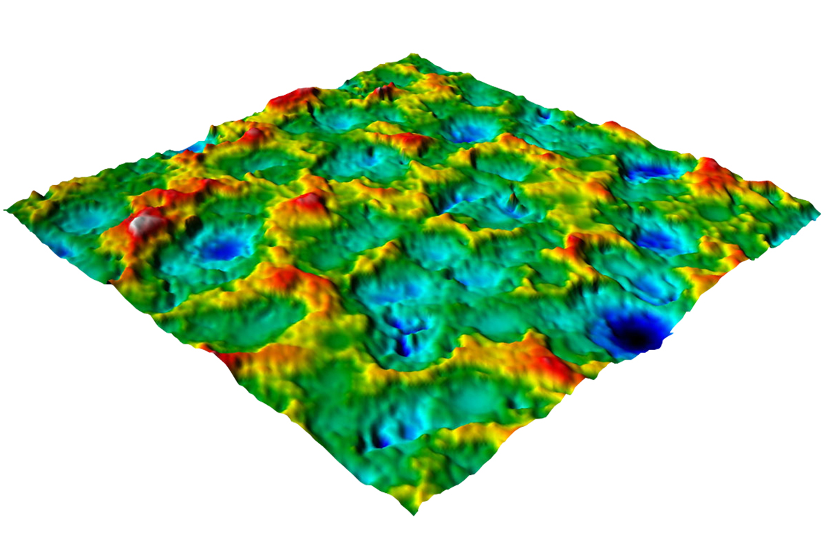
- Contour of a copper surface defect
- Automatic detection of defects using 3D edge finding
- Surface waviness compensation algorithms
 ELECTRICAL CONTACT SURFACE(1)
- Gold surface
- 400 µm range, fast scanning speed
- systems equipped with the confocal microscope (CFM) are well suited for rough and highly contoured surfaces
 ELECTRICAL CONTACT SURFACE(2)
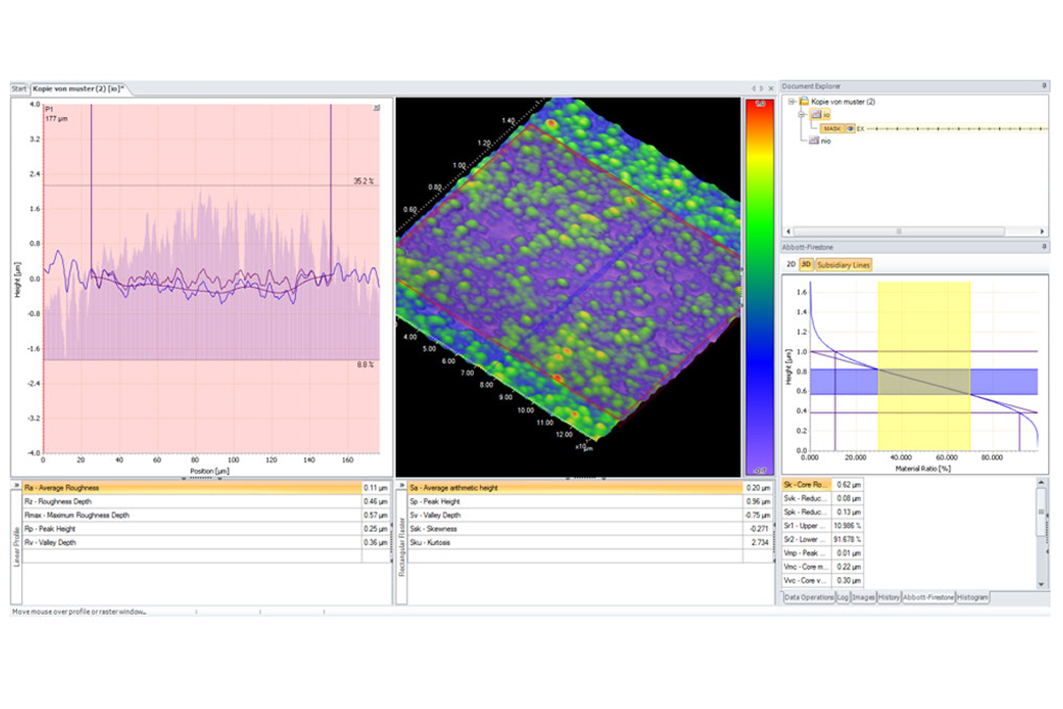
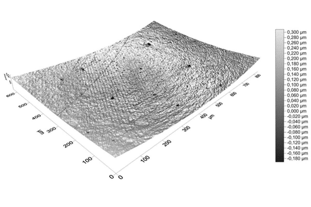
- Roughness of an electrical contact surface
- CFM Scan with 100X magnification, 0,23 µm lateral and 1 nm height resolution
- 2D and 3D roughness, material ratio