


Inquiry
Cart
Laser Equipment - Precision Processing, Innovative Technology
Laser Equipment - Precision Processing, Innovative Technology
TSV Si Wafer Drilling
Semiconductor Industry

TSV Si Wafer Drilling
- With the rapid explosion of AI development in Taiwan, TSV (Through-Silicon Via) serves as a critical connection channel. TSV 3D stacking technology involves wafer drilling, filling conductor vias, and wafer bonding to stack and connect all chip layers.
- Laser Tek TSV Drilling Machine utilizes Femtosecond Laser
- Achieves chip-free edges, no cracks, and no subsurface damage for both front and back holes
- Front/Back hole diameter error < 5μm
Product Description
Other Product Description
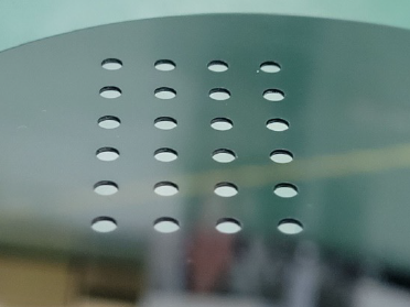
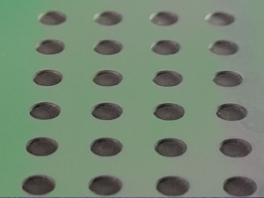
 Through-hole Quality
 Through-hole Quality
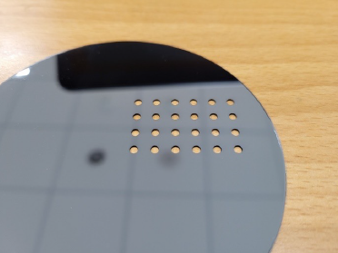
 Polished Surface (Top Side)
 Polished Surface (Top Side)
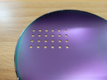
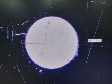 Front/Back hole diameter error < 5μm<br>(Top View)
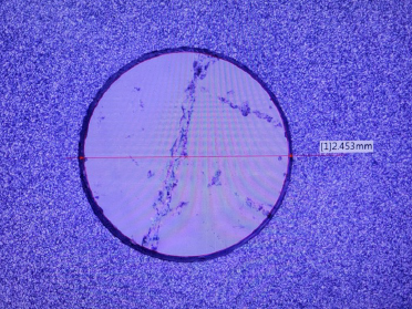 Front/Back hole diameter error < 5μm<br>(Bottom View)
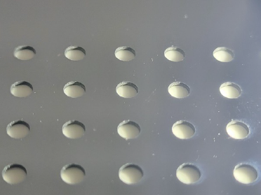
 Blind Hole Quality
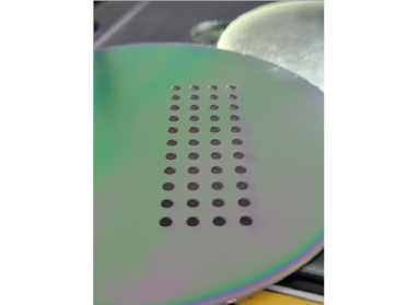 Blind Hole Quality